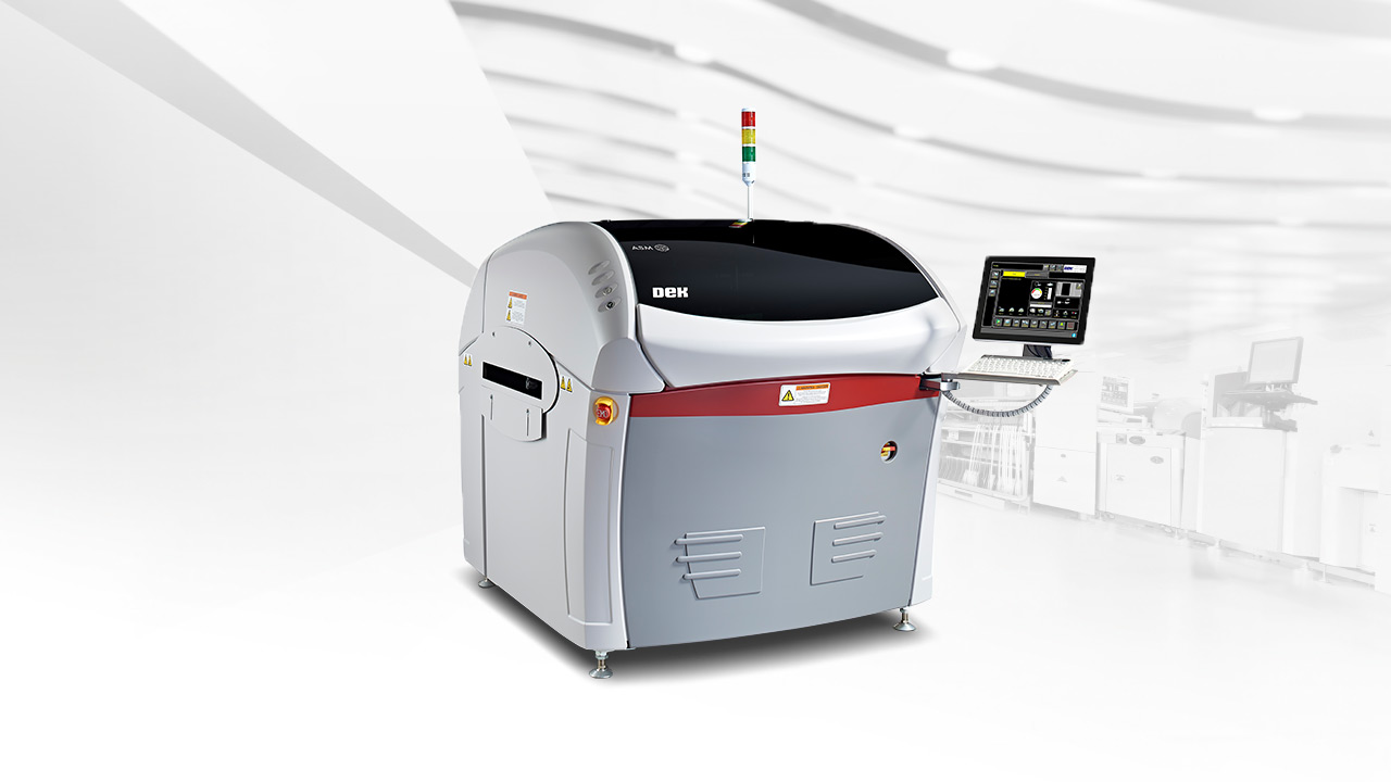
DEK Galaxy
The ideal solution for semiconductor, hybrid and high-end SMT applications
The DEK Galaxy platform brings the superior efficiency and precision of modern printing methods to semiconductor production and hybrid packaging applications. It sets new industry benchmarks for high-tech semiconductor packaging work in terms of throughput, repeatability and efficiency.
High-precision linear drives and powerful camera systems provide the DEK Galaxy with a solid foundation for ultra-fast, ultra-precise performance. With transfer options that support high-precision wafer pallets and the power to print substrates using innovative tool technologies such as DEK's Virtual Panel Tool (VPT), DEK Galaxy can efficiently meet the most demanding requirements. With the DirEKt Ball Placement option, you can achieve highly accurate wafer printing and screen printing processes, including extremely precise wafer bumping and direct placement of solder balls to 0.2mm diameters.
Video
Advantage
- Linear drives for maximum accuracy: ±12.5 @ 2 Cpk Six Sigma repeatability supports the most demanding wafer, substrate and PCB applications
- ProFlow® DirEKt Imaging technology for precise ball placement
- Modular: Enables flexible configuration with tooling and transfer systems to meet the needs of the widest range of wafer and advanced packaging applications
- SMEMA compliant interface supports wafer and flux solutions
- SECS/GEM interface with higher level systems
Product Specifications
- Device alignment accuracy ±12.5 μm @ 2 Cmk
- Process alignment accuracy ±12.5 μm @ 2 Cmk
- Device base time 7 seconds (up to 4 seconds with RTC option)
- Product changeover in less than 2 minutes
- Compliant with the communication protocol of semiconductor factory automation SECS / GEM
- Remote operation, monitoring and diagnostics
- Linear motor technology for optimum speed and precision